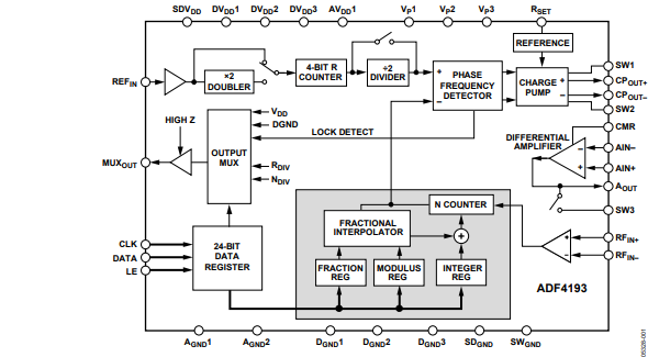
The ADF4193 frequency synthesizer can be used to realize the local oscillator in the up-conversion and down-conversion parts of wireless receivers and transmitters. Its architecture is specifically designed to meet GSM/EDGE lock time base station requirements. It consists of a low noise, digital phase frequency detector (PFD) and a precision differential charge pump.
Principle block diagram

There is also a differential amplifier that converts the differential charge pump output into a single terminal voltage for an external voltage controlled oscillator (VCO). The sigma-δ-based fractional order interpolator, which works in conjunction with the N divider, allows programmable modulo fractional order N division. In addition, a 4-bit reference (R) counter and an on-chip frequency multiplier allow the selection of a reference signal (REFIN) frequency at the PFD input. If the synthesizer is used with an outer loop filter and a VCO, a full PLL (phase locked loop) can be achieved.
The switching architecture ensures that the PLL is stable within the GSM timeslot protection cycle, eliminating the need for a second PLL and associated isolation switch. This reduces cost, complexity, PCB area, shielding, and features of previous Ping-Pong GSM PLL architectures.