TDA7560 Introduction
The TDA7560 is a high-performance Class AB audio power amplifier built using advanced BCD (Bipolar, CMOS, DMOS) technology. Packaged in a Flexiwatt 25 format, it is specifically designed to deliver high power for car radio applications, offering exceptional efficiency and reliability.
This amplifier features a fully complementary P-Channel/N-Channel output stage, enabling a rail-to-rail voltage swing. Combined with its high output current capability and minimized saturation losses, the TDA7560 sets a new standard for power delivery in the car audio domain while achieving remarkably low distortion.

1. TAB: Typically a thermal pad, connected to the ground or a heat sink for heat dissipation.
2. P-GND2: Powerground for the second channel.
3. OUT2-: Negative output for the second channel.
4. ST-BY: Standby control pin; toggles between standby mode and active operation.
5. OUT2+: Positive output for the second channel.
6. VCC: Power supply pin for the IC.
7. OUT1-: Negative output for the first channel.
8. P-GND1: Powerground for the first channel.
9. OUT1+: Positive output for the first channel.
10. SVR: Supply Voltage Reference; typically for biasing internal components.
11. IN1: Input for the first channel.
12. IN2: Input for the second channel.
13. S-GND: Signal ground; used for low-noise signal reference.
14. IN4: Input for the fourth channel.
15. IN3: Input for the third channel.
16. AC-GND: AC ground, often used for decoupling or feedback.
17. OUT3+: Positive output for the third channel.
18. P-GND3: Power ground for the third channel.
19. OUT3-: Negative output for the third channel.
20. VCC: Power supply pin for the IC (repeated).
21. OUT4+: Positive output for the fourth channel.
22. MUTE: Mute control pin; toggles mute function.
23. OUT4-: Negative output for the fourth channel.
24. P-GND4: Powerground for the fourth channel.
25. HSD: High-side driver pin; typically related to switching or protection.
Notes:
- If you are working with the ATDA7560 specifically, consult the device's datasheet for precise details and configuration examples.
- Ensure proper decoupling on VCC pins and maintain separation between signal and power grounds (e.g., S-GND and P-GND) to minimize noise.
TDA7560 Symbol

TDA7560 Footprint

TDA7560 3D Model

TDA7560 Block Diagram

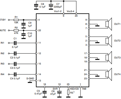
TDA7560 Test and Application Circuit

TDA7560 Specification
| Specification | Details |
| Technology | BCD (Bipolar, CMOS, DMOS) |
| Amplifier Class | Class AB |
| Package | 25-Flexiwatt (Vertical) |
| Number of Channels | 4 |
| Output Configuration | Fully complementary P-Channel/N-Channel |
| Supply Voltage Range | 8V ~ 18V |
| Typical Operating Voltage | 14.4 V |
| Output Power | 50 W x 4 at 4Ω with 14.4 V supply |
| Total Harmonic Distortion (THD) | ≤ 0.02% at 1 W, 4Ω |
| Frequency Response | 20 Hz ~ 20 kHz |
| Quiescent Current | Typically 200 mA |
| Features | Standby, Mute, Diagnostics |
| Rail-to-Rail Swing | Supported |
| Short-Circuit Protection | Built-in |
| Slew Rate | High |
| Operating Temperature | -40°C ~ 85°C |
TDA7560 Features
Multipower BCD technology
MOSFET output power stage
Hi-Fi class distortion
Excellent 2 Ω driving capability
Low output noise
Standby function
Mute function
Automute at min. supply voltage detection
Low external component count:
– Internally fixed gain (26 dB)
– No external compensation
– No bootstrap capacitors
On board 0.35 A high side driver
Protections:
– Output short circuit to GND, to VS, across the load
– Very inductive loads
– Overrating chip temperature with soft thermal limiter
– Output DC offset detection
– Load dump voltage
– Fortuitous open GND
– Reversed battery
– ESD
TDA7560 Applications
SVR (Supply Voltage Rejection):
The SVR capacitor not only enhances ripple rejection but also optimizes pop noise reduction during ON/OFF transitions. A minimum value of 10 µF is recommended.
Input Stage:
The amplifier's inputs are ground-compatible and can handle high input signals up to ±8 V peak without performance degradation.
Input Capacitors:
Standard 0.1 µF input capacitors result in a low-frequency cut-off of approximately 16 Hz, suitable for high-fidelity audio.
Standby and Muting:
Both functions are CMOS-compatible. A 470 kΩ resistance and RC cells are needed to smooth transitions, ensuring noise-free operation. Standby transitions should not exceed 2.5 V/ms.
DC Offset Detector:
Integrated to prevent dangerous DC offsets that can damage speakers. It requires a 10 kΩ pulldown resistor on the HSD pin for proper operation.
Heatsink Requirements:
Under 4Ω speaker load, typical dissipation is 26 W in worst-case scenarios. To prevent thermal shutdown at 70°C ambient temperature, a heatsink with thermal resistance of 2 °C/W is advised.
TDA7560 Package
The TDA7560's 25-Flexiwatt (Vertical) package is a compact and efficient design. With dimensions of 31.3 mm × 10.2 mm and a vertical mounting style, it saves PCB space while providing excellent thermal dissipation, effectively meeting high-performance requirements. Its heatsink is electrically isolated from the ground, ensuring ease of installation and system integration.
In terms of electrical parameters, this package supports the TDA7560's rail-to-rail output swing and typical power dissipation of up to 26W. Combined with a 4Ω speaker load, the amplifier can deliver up to 50W peak output power in bridge mode, making it an ideal solution for high-power car audio systems.

FAQs
What is the TDA7560?
The TDA7560 is a high-power Class AB audio amplifier designed using BCD (Bipolar/CMOS/DMOS) technology.
Does the TDA7560 have protection features?
Yes, the TDA7560 includes thermal shutdown, short-circuit protection, and a DC offset detector to prevent damage to the amplifier or speakers.
How does the TDA7560 manage overheating?
The TDA7560 requires a heatsink with a thermal resistance of approximately 2°C/W to prevent thermal shutdown under continuous high-power operation.